Section 1.6: Logic Gates and Levels #
An amplifier should key up only when the radio asks and its protection circuit sees no fault. An AND gate enforces that rule: it gives a 1 only when both of its inputs are 1. A cooling fan may need a different rule: run when either a switch or a temperature sensor requests it. Which gate you choose depends on how those conditions should combine.
Rules for Ones and Zeros #
Inside the circuit, each 1 or 0 is a voltage, and a convention sets which level stands for which.
Key Information: In positive logic, a high voltage represents 1 and a low voltage represents 0.
This section uses positive logic. “Positive” names the convention, not the polarity of the voltages; negative logic reverses it.
Let 1 mean “run the fan” and 0 mean “no request.” Either request should start the fan, and receiving both should keep it running. An OR gate applies that rule.
NOT reverses a result, changing 1 to 0 and 0 to 1. NAND applies NOT to the AND result; NOR applies it to the OR result.
We can also compare two bits, such as a stored bit and a received bit. An exclusive OR gate, or XOR, gives 1 when one and only one input is 1, meaning the bits differ. An exclusive NOR gate, or XNOR, inverts that result, which makes it a match detector.
To check exactly what each gate does, we can list every input combination with its result. Two inputs, A and B, have four possible combinations. Read across a row to compare the gates:
| A | B | AND | OR | NAND | NOR | Exclusive OR | Exclusive NOR |
|---|---|---|---|---|---|---|---|
| 0 | 0 | 0 | 0 | 1 | 1 | 0 | 1 |
| 0 | 1 | 0 | 1 | 1 | 0 | 1 | 0 |
| 1 | 0 | 0 | 1 | 1 | 0 | 1 | 0 |
| 1 | 1 | 1 | 1 | 0 | 0 | 0 | 1 |
Key Information:
- A truth table lists inputs and their corresponding outputs for a digital device.
- An OR gate produces 1 if any input is 1.
- A NAND gate produces 0 only if all inputs are 1.
- A two-input exclusive NOR gate produces 0 if one and only one input is 1.
Symbols Show the Operation #
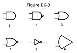
On a schematic, each gate’s symbol shows which rule it applies. An AND symbol has a flat input side and a rounded, D-shaped body. An OR symbol has a curved input side and comes to a point at the output. A small circle, or bubble, on an output means inversion: it changes an AND symbol to NAND or an OR symbol to NOR. That little bubble is easy to miss, and it reverses every result. An inverter uses a triangle with an output bubble.
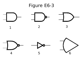
Key Information: In Figure E6-3, symbol 2 is NAND, symbol 4 is NOR, and symbol 5 performs NOT, or inversion.
Logic Has Electrical Limits #
Behind each symbol sits a small transistor circuit. Its construction, called the logic family, sets how much power a gate uses, how well it ignores noise, and what load it can drive.
A battery-powered controller needs logic that draws as little current as possible. In CMOS (complementary metal-oxide-semiconductor) logic, each gate pairs N-channel and P-channel MOSFETs. In either steady state, one device of each pair is off, so almost no current flows from supply to ground. Switching still takes energy to charge and discharge capacitance. Other families, such as TTL (including its faster Schottky versions), emitter-coupled logic (ECL), and NMOS, draw current even while their outputs hold steady.
Noise on an input or power supply should not turn “off” into “on,” and the transmitter a few feet away can supply plenty of it. A gate reads an input as high or low by comparing it with a switching threshold. The farther that threshold sits from both the normal low and high levels, the more a noisy input can rise or fall without changing the interpreted state. That tolerance is a noise margin. Exact input levels vary among CMOS families.
Sometimes a gate needs to accept a signal without drawing much input current, yet drive a load at its output. BiCMOS combines bipolar and CMOS circuitry to do both.
Key Information:
- The CMOS digital logic family has the lowest power consumption.
- CMOS has high immunity to input or supply noise because its input switching threshold is about half the supply voltage.
- BiCMOS offers the high input impedance of CMOS and the low output impedance of bipolar transistors.
Letting Go of a Shared Wire #
Devices sharing a signal wire must take turns driving it, like stations on a net. Otherwise, one output could try to hold the wire high while another holds it low. A control signal can switch a waiting device’s output into a high-impedance state, so another device can drive the line.
In the high-impedance state, the output effectively disconnects. It lets go of the wire rather than sending a third number. When nobody drives the line, however, an input still needs a defined voltage. Noise or leakage could otherwise determine its apparent state. A resistor to one of the supply lines can provide that voltage yet still let an active output override it.
Key Information:
- Tri-state logic has 0, 1, and high-impedance output states.
- A pull-up or pull-down resistor connects to the positive or negative supply to establish a voltage when an input or output is an open circuit.
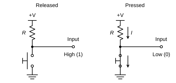
For example, connect a pushbutton between an input and ground, with a pull-up resistor from the input to the positive supply, as drawn below. Released, the button leaves the resistor to establish a high level. Pressed, it connects the input to ground and establishes a low level. The resistor limits current to prevent a short circuit when you press the button.



 High voltage represents a 1, low voltage a 0