

Section 3.2: Amplifier Circuits #
An amplifier’s class describes how much of each signal cycle its device conducts. Class A conducts for all of it and is the most linear; Class C conducts for less than half, trading linearity for efficiency. That one choice decides how clean the output is and how hot the heat sink runs. The class comes from the circuit around the device, especially its bias.
Reading a Transistor Stage #
Figure E7-1 shows a typical NPN transistor stage.
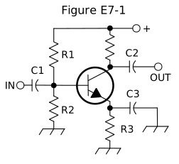
The signal enters the base through C1 and leaves the collector through C2. The unlabeled resistor from the supply to the collector is the collector load; the output voltage develops across it. C3 bypasses the emitter to ground for signals, so the emitter is the terminal the input and output circuits share. Amplifier circuits take their names from that common terminal.
R1 and R2 divide the supply voltage to hold the base at a steady DC voltage, even with no signal. That sets the transistor’s resting point, and R3 holds it steady.
If emitter current rises, perhaps as the transistor warms, the voltage across R3 rises too. With the base voltage fixed by the divider, less voltage remains between base and emitter, which pulls the current back down. The transistor’s own emitter current produces this correction.
R3’s correction is feedback: part of a circuit’s output or response returned to its input. Negative feedback like R3’s opposes a change; positive feedback reinforces one. C3 bypasses R3 for signals, so this feedback doesn’t also cut the signal’s gain.
Key Information:
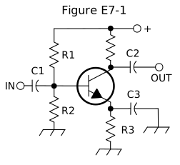
- The amplifier circuit shown in Figure E7-1 is a common-emitter amplifier.
- In Figure E7-1, the purpose of R1 and R2 is voltage divider bias.
- In Figure E7-1, the purpose of R3 is self bias.
When the input drives the base more positive, collector current rises, the drop across the collector load grows, and the collector voltage falls. The stage inverts the signal.
Moving the shared terminal changes that. An emitter follower connects its collector straight to the supply, whose steady voltage acts as ground for signals. That makes the collector the shared terminal, which gives the circuit its other name: common-collector amplifier. The signal still enters the base, but the output comes from the emitter, which has no bypass capacitor. Raise the base voltage, and the emitter voltage rises by nearly the same amount, so the voltage gain is near one. The follower can still supply far more current than it draws from its source.
Tubes offer a similar choice of common terminal. A grounded-grid amplifier, the tube version of common base, holds the grid at RF ground, drives the cathode, and takes the output from the plate. The driving stage must supply the tube’s whole cathode current at a modest voltage, and impedance is voltage divided by current.
Key Information:
- A characteristic of an emitter follower, or common-collector, amplifier is that its input and output signals are in phase.
- A characteristic of a grounded-grid amplifier is low input impedance.
Conduction Angle #
Biased partly on, the stage in Figure E7-1 can run Class A, conducting through all 360 degrees. Its resting point must leave room for the signal to swing both ways. Too far one way is cutoff, where conduction stops. Too far the other is saturation: fully on, with the collector voltage unable to fall further.
Key Information: The operating point of a Class A common-emitter amplifier is approximately halfway between saturation and cutoff.
That bias current flows even with no signal, so a Class A stage runs warm while nobody is talking. A push-pull amplifier divides the waveform between two active elements instead. In Class B, each conducts for exactly half the cycle, and the handoff near the zero crossing can distort the signal. Class AB biases each device slightly on, so their halves overlap and the handoff is smooth.
Class C conducts in pulses shorter than half a cycle. A tuned output circuit rebuilds a sine wave from those current pulses, which works for FM, whose amplitude stays constant. SSB phone is different: its changing amplitude carries the speech, and Class C’s pulses don’t follow it in proportion. Those errors add new frequencies, like the splatter from an overdriven transmitter.
Key Information:
- Each active element in a push-pull Class AB amplifier conducts for more than 180 degrees but less than 360 degrees of the signal cycle.
- The likely result of using a Class C amplifier to amplify a single-sideband phone signal is signal distortion and excessive bandwidth.
Switching for Efficiency #
A switching amplifier takes Class C’s idea further: its device is either fully off, at cutoff, or fully on, at saturation (called the ohmic region for MOSFETs). A device dissipates power when it has voltage across it and current through it at once. Off, the current is small; fully on, the voltage drop is small. Either way, one factor in is small, so little power becomes heat.
A switching waveform has sharp edges, which make it rich in harmonics. Those are the same unwanted signals the previous section’s low-pass networks keep off the air.
Key Information:
- A Class D amplifier uses switching technology to achieve high efficiency.
- Switching amplifiers are more efficient than linear amplifiers because the switching device is at saturation or cutoff most of the time.
- An RF switching amplifier requires a filter at its output to remove harmonic content.
Stopping an Accidental Oscillator #
Not every feedback path is designed in. Stray capacitance, wiring, or magnetic coupling can carry some output back to the input. At some frequency, that stray feedback may arrive in phase and turn positive. With enough gain, the amplifier then oscillates on its own, often far from its working frequency, where you may not notice until someone else does.
Two remedies attack that feedback. A parasitic suppressor, such as a ferrite bead from Chapter 1, damps the unwanted path at the oscillation frequency but has little effect at the working frequency. Neutralization feeds back an opposing signal that cancels the unwanted feedback.
Key Information: Installing parasitic suppressors and/or neutralizing the stage can prevent unwanted oscillations in an RF power amplifier.




 Common emitter